| 欧盟RoHS指令 | Compliant with Exemption |
| 美国出口管制分类ECCN编码 | EAR99 |
| 环保无铅 | LTB |
| 美国海关商品代码 | 8541.29.00.95 |
| SVHC | Yes |
| SVHC超标 | Yes |
| Automotive | Yes |
| PPAP | Unknown |
| 产品类别 | Power MOSFET |
| Configuration | Single |
| Channel Mode | Enhancement |
| Channel Type | P |
| Number of Elements per Chip | 1 |
| Maximum Drain-Source Voltage (V) | 40 |
| Maximum Gate-Source Voltage (V) | 5 |
| Maximum Gate Threshold Voltage (V) | 2.2 |
| Operating Junction Temperature (°C) | -55 to 175 |
| Maximum Continuous Drain Current (A) | 80 |
| Maximum Gate-Source Leakage Current (nA) | 100 |
| Maximum IDSS (uA) | 1 |
| Maximum Drain-Source Resistance (mOhm) | 7.9@10V |
| Typical Gate Charge @ Vgs (nC) | 71@10V |
| Typical Gate Charge @ 10V (nC) | 71 |
| Typical Input Capacitance @ Vds (pF) | 4177@25V |
| Maximum Power Dissipation (mW) | 75000 |
| Typical Fall Time (ns) | 35 |
| Typical Rise Time (ns) | 11 |
| Typical Turn-Off Delay Time (ns) | 42 |
| Typical Turn-On Delay Time (ns) | 12 |
| Minimum Operating Temperature (°C) | -55 |
| Maximum Operating Temperature (°C) | 175 |
| Packaging | Tape and Reel |
| Typical Drain-Source Resistance @ 25°C (mOhm) | 6.5@10V|6.8@10V|9.6@4.5V|9.9@4.5V |
| Maximum Pulsed Drain Current @ TC=25°C (A) | 280 |
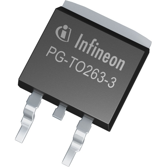
| Mounting | Surface Mount |
| Package Height | 4.4 mm |
| Package Width | 9.25 mm |
| Package Length | 10 mm |
| PCB changed | 2 |
| Tab | Tab |
| Standard Package Name | TO |
| Supplier Package | D2PAK |
| Pin Count | 3 |

