| Not Compliant | |
| EAR99 | |
| Active | |
| 8473.30.11.80 | |
| Automotive | No |
| PPAP | No |
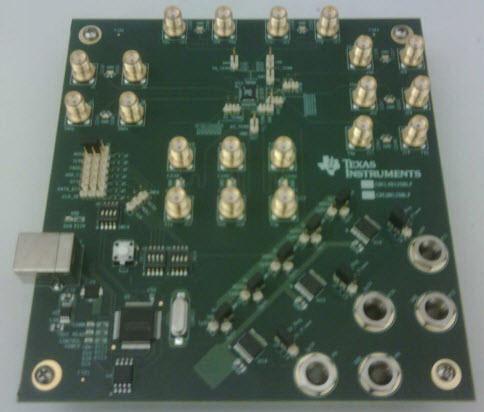
| Evaluation Board | |
| CDCUN1208LP | |
| Clock Buffer and Driver | |
| 400(Max) | |
| USB | |
| 1.8/2.5/3.3 |
Dev Kit Description
The CDCUN1208LP is a 2:8 fan-out buffer featuring a wide operating supply range, two universal differential/ single ended inputs, and universal outputs (HCSL, LVDS, or LVCMOS) with clock edge rate control. One of the device inputs includes a divider that provides divide values of /1, /2, /4, and /8.
The device is offered in a 32 pin QFN package. The CDCUN1208LP is flexible and easy to use. The application configures the device by setting the state of certain pins at device power-up. Alternately, the application can configure the device via SPI/I2C. The CDCUN1208LP delivers excellent additive jitter performance, and low power consumption. The output section includes four dedicated output supply pins enabling the operation of output ports from different power supply domains. This provides the ability to clock devices switching at different LVCMOS levels without the need for external logic level translation circuitry.
设计 AI 驱动的医疗设备
阅读 Arrow 白皮书,掌握系统设计技巧、器件推荐与 AI 洞察,助力高效、安全打造医疗方案。

