| RoHS (Unión Europea) | Compliant with Exemption |
| ECCN (Estados Unidos) | EAR99 |
| Estatus de pieza | Active |
| Código HTS | 8541.29.00.95 |
| SVHC | Yes |
| Índice de SEP por encima del límite autorizado | Yes |
| Automotive | No |
| PPAP | No |
| Categoría del producto | Power MOSFET |
| Configuration | Single Quad Drain Triple Source |
| Channel Mode | Enhancement |
| Channel Type | P |
| Number of Elements per Chip | 1 |
| Maximum Drain-Source Voltage (V) | 150 |
| Maximum Gate-Source Voltage (V) | ±20 |
| Maximum Gate Threshold Voltage (V) | 4 |
| Operating Junction Temperature (°C) | -55 to 150 |
| Maximum Continuous Drain Current (A) | 37 |
| Maximum Gate-Source Leakage Current (nA) | 100 |
| Maximum IDSS (uA) | 1 |
| Maximum Drain-Source Resistance (mOhm) | 47.5@10V |
| Typical Gate Charge @ Vgs (nC) | 25@7.5V|31.8@10V |
| Typical Gate Charge @ 10V (nC) | 31.8 |
| Typical Gate to Drain Charge (nC) | 9.5 |
| Typical Gate to Source Charge (nC) | 9.2 |
| Typical Reverse Recovery Charge (nC) | 245 |
| Typical Input Capacitance @ Vds (pF) | 1805@75V |
| Typical Reverse Transfer Capacitance @ Vds (pF) | 14.5@75V |
| Minimum Gate Threshold Voltage (V) | 2 |
| Typical Output Capacitance (pF) | 332 |
| Maximum Power Dissipation (mW) | 6250 |
| Typical Fall Time (ns) | 9 |
| Typical Rise Time (ns) | 7 |
| Typical Turn-Off Delay Time (ns) | 28 |
| Typical Turn-On Delay Time (ns) | 15 |
| Minimum Operating Temperature (°C) | -55 |
| Maximum Operating Temperature (°C) | 150 |
| Packaging | Tape and Reel |
| Typical Drain-Source Resistance @ 25°C (mOhm) | 60@6V|55@7V|50@8V|45@9V|40@10V |
| Maximum Power Dissipation on PCB @ TC=25°C (W) | 6.25 |
| Maximum Pulsed Drain Current @ TC=25°C (A) | 50 |
| Maximum Junction Ambient Thermal Resistance on PCB (°C/W) | 54 |
| Typical Diode Forward Voltage (V) | 0.79 |
| Typical Gate Plateau Voltage (V) | 5.5 |
| Typical Reverse Recovery Time (ns) | 75 |
| Maximum Diode Forward Voltage (V) | 1.1 |
| Minimum Gate Resistance (Ohm) | 1.9 |
| Maximum Gate Resistance (Ohm) | 6 |
| Maximum Positive Gate-Source Voltage (V) | 20 |
| Maximum Continuous Drain Current on PCB @ TC=25°C (A) | 9 |
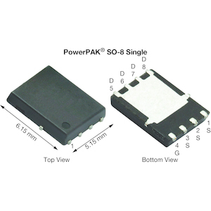
| Mounting | Surface Mount |
| Package Height | 1.07(Max) mm |
| Package Width | 5.89 mm |
| Package Length | 4.9 mm |
| PCB changed | 8 |
| Standard Package Name | SO |
| Supplier Package | PowerPAK SO EP |
| Pin Count | 8 |
| Lead Shape | No Lead |

