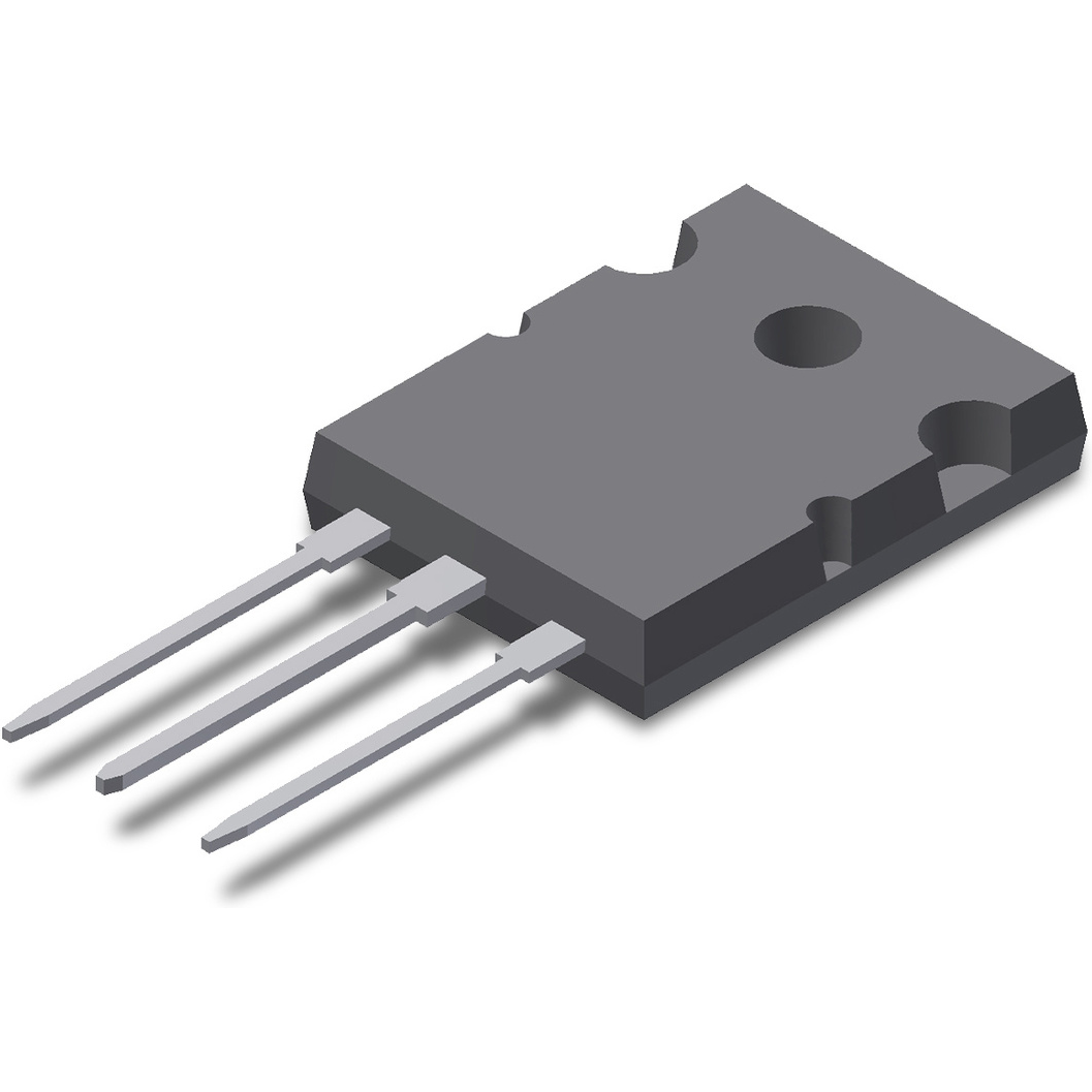
| EU RoHS | Compliant with Exemption |
| ECCN (US) | EAR99 |
| Part Status | Active |
| HTS | 8541.29.00.95 |
| SVHC | Yes |
| SVHC Exceeds Threshold | Yes |
| Automotive | No |
| PPAP | No |
| Product Category | Power MOSFET |
| Configuration | Single |
| Channel Mode | Enhancement |
| Channel Type | N |
| Number of Elements per Chip | 1 |
| Maximum Drain-Source Voltage (V) | 100 |
| Maximum Gate-Source Voltage (V) | ±20 |
| Maximum Gate Threshold Voltage (V) | 4.5 |
| Operating Junction Temperature (°C) | 150 |
| Maximum Continuous Drain Current (A) | 200 |
| Maximum Gate-Source Leakage Current (nA) | 200 |
| Maximum IDSS (uA) | 10 |
| Maximum Drain-Source Resistance (mOhm) | 11@10V |
| Typical Gate Charge @ Vgs (nC) | 540@10V |
| Typical Gate Charge @ 10V (nC) | 540 |
| Typical Gate to Drain Charge (nC) | 226 |
| Typical Gate to Source Charge (nC) | 115 |
| Typical Reverse Recovery Charge (nC) | 3000 |
| Typical Input Capacitance @ Vds (pF) | 23000@25V |
| Typical Reverse Transfer Capacitance @ Vds (pF) | 610@25V |
| Minimum Gate Threshold Voltage (V) | 2 |
| Typical Output Capacitance (pF) | 3200 |
| Maximum Power Dissipation (mW) | 1040000 |
| Typical Fall Time (ns) | 27 |
| Typical Rise Time (ns) | 225 |
| Typical Turn-Off Delay Time (ns) | 127 |
| Typical Turn-On Delay Time (ns) | 40 |
| Minimum Operating Temperature (°C) | -55 |
| Maximum Operating Temperature (°C) | 150 |
| Maximum Pulsed Drain Current @ TC=25°C (A) | 500 |
| Typical Gate Plateau Voltage (V) | 6 |
| Typical Reverse Recovery Time (ns) | 245 |
| Maximum Diode Forward Voltage (V) | 1.4 |
| Maximum Positive Gate-Source Voltage (V) | 20 |
| Mounting | Through Hole |
| Package Height | 26.16(Max) |
| Package Width | 5.13(Max) |
| Package Length | 19.96(Max) |
| PCB changed | 3 |
| Tab | Tab |
| Standard Package Name | TO |
| Supplier Package | TO-264AA |
| Pin Count | 3 |
| Lead Shape | Through Hole |

