

MOSFETs
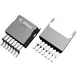
IMBF170R1K0M1XTMA1
CoolSiC™ 1700 V SiC Trench MOSFET in TO-263-7 package | The 650V CoolMOS™ CFD7 superjunction MOSFET with integrated fast body diode in TO-247 package is the perfect choice for resonant high power topologies.
Infineon Technologies AGInfineon’s CoolSiC™ 1700 V, 1000 mΩ SiC MOSFET in a TO-263-7 high creepage package is optimized for fly-back topologies to be used in auxiliary power supplies connected to DC-link voltages 600 V up to 1000 V in numerous power applications.
Summary of Features
- • Optimized for fly-back topologies
- • Extremely low switching loss
- • 12 V / 0 V gate-source voltage compatible with fly-back controllers
- • Fully controllable dV/dt for EMI optimization
- • SMD package with enhanced creepage and clearance distances, > 7 mm
Benefits
- • 1700 V SiC MOSFET enables simple single-ended fly-back topology at high efficiency level for use in auxiliary power supplies
- • SMD package enables direct integration into PCB, with natural convection cooling without extra heatsink
- • Reduced isolation effort due to extended creepage and clearance distances of package
- • Reduced system complexity
- • High power density
Potential Applications
- • Energy Storage Systems
- • Fast EV charging
- • Industrial drives
- • Power Management (SMPS) - Reference Design
- • Solutions for solar energy systems
Related Products
Reference Board: REF_62W_FLY_1700V_SIC
See More New Products From Infineon
Discover More Solutions From Infineon
Product Technical Specifications
EU RoHS
Compliant
ECCN (US)
EAR99
Part Status
Active
HTS
8541.29.00.55
Automotive
Yes
PPAP
Unknown
Category
Power MOSFET
Material
SiC
Configuration
Single Hex Source
Channel Mode
Enhancement
Channel Type
N
Number of Elements per Chip
1
Maximum Drain-Source Voltage (V)
1700
Maximum Gate-Source Voltage (V)
20
Maximum Continuous Drain Current (A)
5.2
Maximum Drain-Source Resistance (mOhm)
880@15V
Typical Gate Charge @ Vgs (nC)
5@12V
Typical Input Capacitance @ Vds (pF)
275@1000V
Maximum Power Dissipation (mW)
68000
Typical Fall Time (ns)
22
Typical Rise Time (ns)
14
Typical Turn-Off Delay Time (ns)
20
Typical Turn-On Delay Time (ns)
19
Minimum Operating Temperature (°C)
-55
Maximum Operating Temperature (°C)
175
Packaging
Tape and Reel
Mounting
Surface Mount
Package Height
4.4
Package Width
9.25
Package Length
10
PCB changed
7
Tab
Tab
Standard Package Name
TO
Supplier Package
TO-263
Pin Count
8
Order Quantity